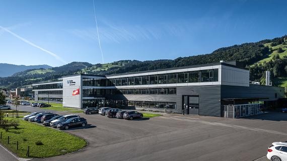
Production process - from the idea to the finished sensor
.

Design
Our consultants and engineers discuss your application's requirements with you to better understand your needs. Perhaps one of our thousands of standard products will suffice, or we make a minor adjustment or create a completely new product.
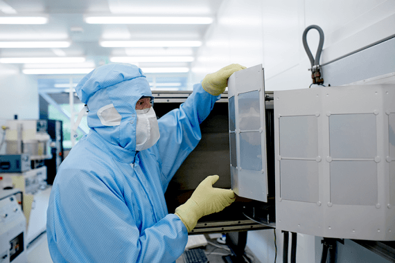
Deposition of substrates
The first production step is deposition, where sputtering is used in order to cover the substrates with a thin layer over the entire surface. Depending on the type of sensor that is required, different materials, thicknesses and qualities can be chosen for the covering.
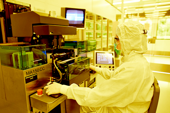
Photolithography
In this step, the substrates are coated with photosensitive lacquer by a centrifuge. All our sensor structures are sketched on so-called masks: through exposure, light is lead through the mask onto the photoresist. The covered parts are not reached by the light, leaving the coating unexposed. During the subsequent developing of the substrates, the coating on the exposed areas is washed away, the non-exposed area remains on the substrate.

Etching
During the etching process the part of the coating that is not required is removed through etching. Two different processes are used to etch the substrates: ion etching and wet-chemical etching.
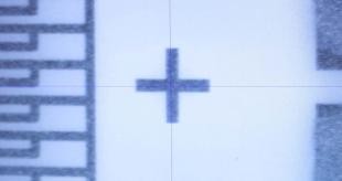
Laser trimming
IST AG uses laser trimming or laser calibration as a method of adjusting (trimming) components by laser induced material changes. Thereby the resistance value is increased continuously by decreasing the meander structure until the desired value is achieved.

Screen printing
During screen printing, the contact points are strengthened with a conductive paste. This enables a better connection between the contact point and the electrical contacts. Additionally, the substrate is covered with a non-conductive paste, which prevents scratches and damages of the sensor due to mechanical or chemical influences.
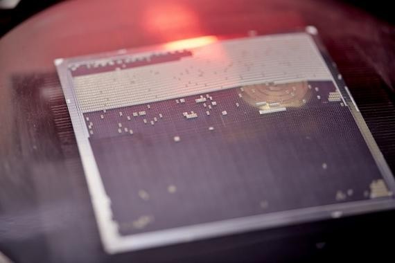
Dicing
While dicing, the substrates are cut into individual strips, so that afterwards wires can be welded on the sensors.
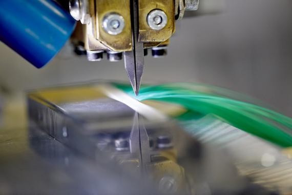
Welding
For the welding process, IST AG offers various possibilities of wire material, lengths and diameters that are welded to the chip. We distinguish between bare and insulated wires. To enhance the welding point and to protect it from mechanical damage, a paste is applied to the welding area offering an outstanding pull-strength.

Measuring
During the final electrical measurement, all sensors are checked. Depending on their classification or assembly they are qualified either with a 2-point calibration measurement or resistance-testing. According to their accuracy they are sorted into different classes.
Our versatile technological portfolio covers different substrate material choices, the use of thin- and thick-film technologies and patterning technologies as well as diverse test and assembly options.
